Place your finger on a glass surface, and within milliseconds, a decision is made: access granted or denied. No passwords to remember, no keys to lose. But behind that split-second unlock lies a sophisticated interplay of physics, electrical engineering, and pattern recognition that most users never consider.
The ridges on your fingertips—formally known as dermatoglyphs—began forming during the third month of fetal development and were fully established by month six. These patterns emerge from a fascinating biological process: epithelial cells undergo a truncated version of hair follicle development, creating raised ridges without actually forming hair. The precise positioning of these ridges is influenced by factors including the mechanical forces within the womb, blood vessel patterns beneath the skin, and random developmental variations. Even identical twins, who share nearly identical DNA, have completely different fingerprints. This uniqueness makes fingerprints one of the most reliable biometric identifiers available.
The Architecture of Recognition
Before understanding how sensors work, we need to understand what they’re looking for. A fingerprint isn’t stored as an image—that would be both inefficient and a privacy nightmare. Instead, recognition systems extract specific features called minutiae.
The two most important minutiae types are ridge endings—where a ridge terminates abruptly—and bifurcations—where a single ridge splits into two branches. A good-quality fingerprint typically contains 25 to 80 minutiae points. When you register your fingerprint, the system records the position, direction, and type of these features. During authentication, it attempts to match these stored minutiae against newly captured ones.
The matching algorithm doesn’t require a perfect overlay. Your finger might be placed at a slightly different angle, or pressure might cause minor distortions. The algorithm accounts for this by using elastic matching techniques that tolerate reasonable geometric transformations while still requiring sufficient corresponding points to declare a match.
Capacitive Sensors: Reading Electrical Fields
The most common fingerprint sensors in smartphones until recently were capacitive. These devices exploit a fundamental principle of electricity: the capacitor.
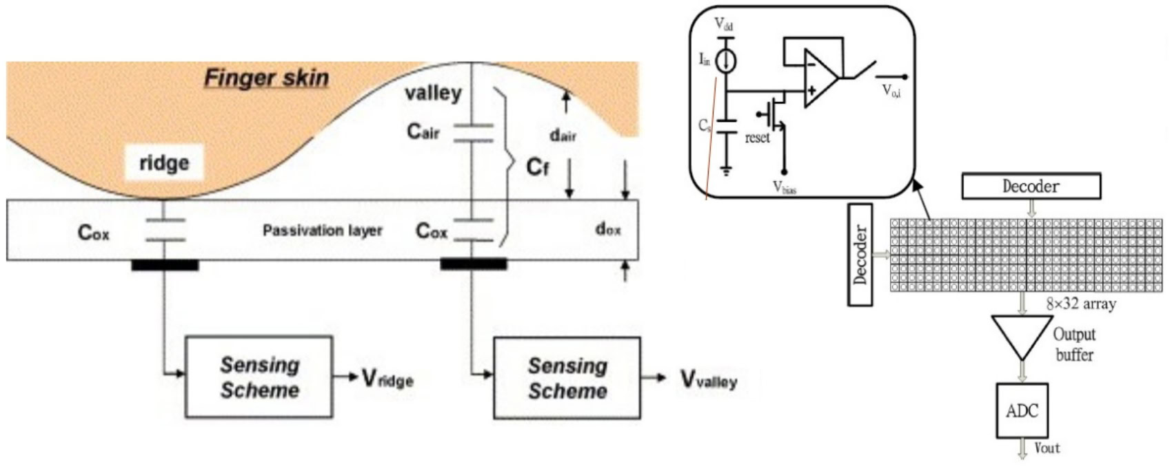
Image source: Android Authority
A capacitive sensor consists of an array of tiny capacitor plates beneath a protective surface. Each capacitor can store a small electrical charge. When your finger touches the sensor, the ridges make direct contact with the surface, while valleys remain separated by air gaps. This difference matters because capacitance depends on the distance between conductive surfaces.
For a ridge touching the surface, the conductive property of your skin—thanks to its water and salt content—changes the capacitance at that location. A valley, with its air gap, leaves the capacitance essentially unchanged. An operational amplifier integrator circuit measures these minute differences across thousands of capacitors, and an analog-to-digital converter transforms the electrical signals into a digital representation.
The resolution of a capacitive sensor is critical. NIST standards specify 500 pixels per inch (PPI) as the minimum for reliable fingerprint identification. At this resolution, each capacitor needs to be smaller than the width of a fingerprint ridge—roughly 100 to 300 micrometers. Modern sensors pack hundreds or thousands of these capacitive elements into a space smaller than a thumbnail.
Capacitive sensors offer significant security advantages. Unlike optical methods that capture a visual image, capacitive sensors measure electrical properties that are difficult to replicate. A photograph or simple printed image won’t work. Even a silicone mold might fail if its electrical properties differ from real skin.
Optical Sensors: The Light-Based Approach
Before capacitive sensors dominated smartphones, optical fingerprint scanners were the standard—and they remain widely used in access control systems and time-attendance terminals.

Image source: Android Authority
An optical sensor operates like a specialized camera. LEDs illuminate your finger pressed against a glass platen. The ridges, making contact with the glass, reflect light differently than the valleys, which are separated by air. A lens system focuses this reflected light onto a CMOS or CCD image sensor, capturing a high-contrast photograph of your fingerprint pattern.
The simplicity of this approach has advantages: optical sensors are relatively inexpensive, durable, and can achieve high resolution. However, they have significant limitations. A high-quality photograph of a fingerprint can potentially fool an optical sensor because it’s essentially looking for visual patterns.
Modern implementations often combine optical sensing with capacitive elements to detect whether a real finger is present, creating hybrid sensors that balance cost with improved security.
Ultrasonic Sensors: Seeing in Three Dimensions
The newest technology in smartphone fingerprint recognition uses sound waves. First introduced in 2016 and popularized in premium devices, ultrasonic sensors represent a significant leap forward in both security and versatility.
An ultrasonic sensor works like a miniature sonar system. Piezoelectric micromachined ultrasonic transducers (PMUTs) emit high-frequency sound pulses toward your finger. These sound waves, typically around 22 MHz, penetrate the outer layer of skin. When they encounter boundaries between materials of different acoustic impedance—like the interface between skin and air in a valley—they reflect back.
The sensor measures both the timing and intensity of these returning echoes. Ridges, being closer, return echoes faster than valleys. This time-of-flight information allows the system to construct a three-dimensional map of the fingerprint surface. Some systems can even capture subdermal features, reading the internal fingerprint structure beneath the surface layer of skin.
This 3D capability provides significant advantages:
Works through contaminants: Light oil, moisture, or dirt that might confuse optical or capacitive sensors is transparent to ultrasonic waves.
Integrates under displays: The sensor can sit behind an OLED screen, emitting sound waves through the display glass. This enables the sleek in-display fingerprint readers on modern smartphones.
Resists spoofing: Because ultrasonic sensors read depth information and can potentially capture subsurface features, they’re more resistant to fake fingerprints made from silicone, gelatin, or other materials.
The trade-offs include higher cost, more complex signal processing, and in some early implementations, slightly slower unlock times compared to capacitive sensors. Second-generation ultrasonic sensors have improved speed significantly while expanding the sensing area, allowing for more reliable one-touch unlocks.
The Matching Pipeline
Capturing a fingerprint is only half the battle. The system must then process and match it against stored templates. This pipeline involves several sophisticated steps.
Image Enhancement: Raw fingerprint captures are rarely perfect. Sensors apply filters to enhance contrast between ridges and valleys. The Gabor filter is particularly effective because it can enhance ridges oriented in a specific direction while suppressing noise, following the natural flow of ridge patterns.
Binarization: The enhanced grayscale image is converted to black and white, where each pixel is classified as either ridge or valley.
Thinning: Ridges are reduced to single-pixel width through skeletonization, making subsequent minutiae extraction more accurate.
Minutiae Extraction: The system identifies ridge endings, bifurcations, and other distinctive features. The “crossing number” method is commonly used—scanning a 3×3 window around each pixel to count how many times the ridge crosses the window boundary. A crossing number of 1 indicates a ridge ending; 3 indicates a bifurcation.
Template Generation: The positions, orientations, and types of minutiae are encoded into a compact mathematical template, typically just a few hundred bytes.
Matching: During authentication, the algorithm compares the newly extracted minutiae against stored templates. It must handle rotation, translation, and slight distortions while ensuring enough corresponding points to declare a match. Most systems require at least 12-16 matching minutiae for positive identification, though the exact threshold varies by application.
Security Architecture: Where Your Fingerprint Lives
A critical question often overlooked: where exactly is your fingerprint data stored? The answer reveals a sophisticated security architecture designed to protect biometric data from extraction.
Your fingerprint template doesn’t reside in the regular file system where apps could potentially access it. Instead, modern smartphones use a Trusted Execution Environment (TEE)—a secure area of the main processor that runs isolated from the main operating system. The TEE handles all biometric processing and stores the encrypted templates in protected memory.
Apple calls this the “Secure Enclave,” while Qualcomm uses “Secure Processing Unit (SPU).” By whatever name, the principle is the same: even if malware compromises the main operating system, it cannot directly access fingerprint data or the matching process.
When you authenticate:
- The fingerprint sensor sends encrypted data to the TEE
- The TEE performs the matching against stored templates
- The TEE returns only a yes/no decision to the main processor
- The actual fingerprint template never leaves the secure environment
This architecture also enables FIDO (Fast IDentity Online) authentication. When you use your fingerprint to log into a website, your fingerprint data never leaves your phone. Instead, the TEE signs a challenge from the server using a private key, and the server verifies the signature. Your biometric data stays entirely local.
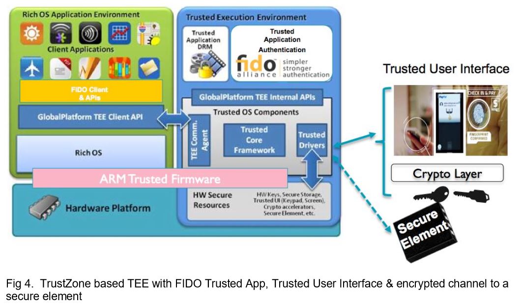
Image source: Android Authority
The Numbers Game: Accuracy Metrics
Biometric systems are evaluated using two critical metrics that represent a fundamental trade-off:
False Acceptance Rate (FAR): The probability that the system incorrectly grants access to an unauthorized person. A FAR of 1 in 50,000 means there’s a 0.002% chance that a random person’s fingerprint could unlock your device.
False Rejection Rate (FRR): The probability that the system incorrectly denies access to the legitimate owner. An FRR of 2% means you’ll need to try twice about 1 time in 50.
These metrics are inversely related. Lowering the FAR (making the system more secure) typically increases the FRR (making it more annoying for legitimate users). System designers must balance security against usability based on the application.
Modern smartphone fingerprint sensors typically achieve FAR around 1 in 50,000 with FRR under 2%. For higher-security applications like border control or financial transactions, more stringent thresholds may be required.
The Spoofing Arms Race
No security system is impenetrable, and fingerprint recognition is no exception. Researchers have demonstrated various attack methods:
Direct spoofing: Creating artificial fingerprints from materials like gelatin, silicone, or latex. Early optical sensors were particularly vulnerable. Capacitive sensors raised the bar by requiring similar electrical properties. Ultrasonic sensors add depth information, making spoofing even more difficult.
Presentation attacks: Using high-resolution photographs or latent prints lifted from surfaces. The famous 2013 demonstration of defeating an iPhone 5s fingerprint sensor using a lifted print highlighted this vulnerability.
Reconstruction attacks: Using the mathematical template (if obtained) to reconstruct a synthetic fingerprint that matches. This is why template protection is so critical.
Defense mechanisms include liveness detection—algorithms that check for signs of life like skin conductivity, pulse detection, or the natural distortion patterns of a pressed finger. More sophisticated systems analyze sweat pores, which are difficult to replicate in artificial materials.
In-Display Revolution
The demand for bezel-less smartphones drove innovation in fingerprint sensor placement. Capacitive sensors required exposed surface area, but in-display sensors could hide beneath the screen.
Two approaches emerged:
Optical in-display sensors use the phone’s display as a light source, flashing the screen to illuminate the finger while a camera beneath the OLED panel captures the reflected pattern. These are cost-effective but inherit optical vulnerabilities.
Ultrasonic in-display sensors send sound waves through the display glass. Qualcomm’s second-generation 3D Sonic Sensor increased the sensing area by 77%, making it easier to unlock without precise finger placement. The larger sensor can even capture enough detail for two-finger authentication.
Both technologies require careful integration with the display assembly, but ultrasonic’s ability to work through thicker glass and resist contamination has made it the preferred choice for premium devices.
From Crime Labs to Pocket Computers
The journey of fingerprint recognition from forensic tool to consumer convenience is remarkable. The first automated fingerprint identification system (AFIS) was developed in the 1960s, with the FBI launching IAFIS (Integrated Automated Fingerprint Identification System) in 1999. These massive systems processed fingerprint cards at scale, searching databases of millions of prints.
The miniaturization required to put a fingerprint sensor on a smartphone—achieving comparable accuracy in a device the size of a button—represents decades of engineering progress. Capacitive arrays shrank from centimeters to millimeters. Signal processing algorithms became efficient enough to run on mobile processors. Secure hardware enclaves made biometric storage safe enough for consumer devices.
Looking Forward
Fingerprint recognition continues to evolve. Researchers are exploring:
Contactless sensing: Capturing fingerprints without physical contact using high-resolution cameras, useful in hygiene-sensitive environments.
Multispectral imaging: Reading fingerprints at various wavelengths to capture both surface and subsurface features, improving robustness and security.
Continuous authentication: Using fingerprint sensors to verify identity continuously during device use, not just at unlock.
Integration with other biometrics: Combining fingerprints with facial recognition, iris scanning, or behavioral biometrics for multi-factor authentication.
The fundamental physics remains constant: your fingerprints are unique, permanent, and can be measured. The technologies we use to capture and match them will keep advancing, but the basic principle—matching the ridges and valleys that formed before you were born—remains the foundation of this ubiquitous security technology.
References
- NIST Fingerprint Image Quality 2 (NFIQ 2). National Institute of Standards and Technology. NIST IR 8382, 2021.
- Maltoni, D., Maio, D., Jain, A.K., & Prabhakar, S. Handbook of Fingerprint Recognition. Springer, 2009.
- Qualcomm 3D Sonic Sensor Technology. Qualcomm Technologies, Inc. Technical Documentation, 2019-2024.
- ISO/IEC 19794-2:2011. Biometric Data Interchange Formats - Part 2: Finger Minutiae Data. International Organization for Standardization.
- FIPS 201-3. Personal Identity Verification (PIV) of Federal Employees and Contractors. NIST, 2022.
- Gomez, F., et al. “Ultrasonic Fingerprint Sensor Using a Piezoelectric Micromachined Ultrasonic Transducer Array.” IEEE Journal of Solid-State Circuits, 2015.
- MedlinePlus Genetics. “Are Fingerprints Determined by Genetics?” National Library of Medicine, 2022.
- Headon, R., et al. “The Developmental Basis of Fingerprint Pattern Formation and Variation.” Cell, 2023.
- Android Authority. “How Fingerprint Scanners Work: Optical, Capacitive, and Ultrasonic Explained.” 2025.
- Bayometric. “Minutiae Based Extraction in Fingerprint Recognition.” Technical Documentation, 2016.