On April 25, 1954, three scientists at Bell Laboratories in Murray Hill, New Jersey, demonstrated something that would eventually reshape the global energy landscape. Daryl Chapin, Calvin Fuller, and Gerald Pearson held a press conference to showcase the first practical silicon solar cell—a device that converted sunlight directly into electricity with 6% efficiency. To prove it worked, they used the cell to power a small toy Ferris wheel spinning under a lamp.
The New York Times covered the announcement with cautious optimism: “The silicon solar cell may be recognized eventually as one of the most significant developments of the 20th century.” Seven decades later, with global solar capacity exceeding 1,500 gigawatts and panels approaching 25% commercial efficiency, that prediction has proven remarkably accurate.
But how does a piece of silicon turn photons into electrons? The answer involves quantum mechanics, semiconductor physics, and one of the most elegant applications of the P-N junction ever engineered.
The Photovoltaic Effect: Where Light Meets Matter
The fundamental principle behind solar cells was discovered 115 years before Bell Labs’ demonstration. In 1839, a 19-year-old French physicist named Edmond Becquerel was experimenting with electrolytic cells in his father’s laboratory. He observed that exposing certain materials to light generated a small electric current—the first documented observation of the photovoltaic effect.
What Becquerel witnessed was a quantum interaction between light and matter. Photons—packets of electromagnetic energy—carry energy proportional to their frequency, described by Max Planck’s equation:
$$E = hf$$where $E$ is photon energy, $h$ is Planck’s constant, and $f$ is frequency. When a photon strikes a semiconductor material, one of three things happens: the photon passes through, reflects off the surface, or gets absorbed. Absorption is what matters for solar cells.
For absorption to occur, the photon’s energy must exceed the material’s band gap—the minimum energy required to excite an electron from the valence band (where it’s bound to an atom) to the conduction band (where it can move freely). Silicon’s band gap is 1.12 electron volts (eV), which corresponds to photons with wavelengths shorter than about 1,100 nanometers—infrared light. Any photon with energy above this threshold can potentially create an electron-hole pair.

Image source: Wikipedia - Theory of solar cells
When a photon with sufficient energy strikes a silicon atom, it transfers its energy to an electron in the valence band. If this energy exceeds the band gap, the electron jumps to the conduction band, leaving behind a “hole”—the absence of an electron where one previously existed. This hole behaves like a positively charged particle, capable of moving through the crystal lattice as adjacent electrons fill the vacancy.
The P-N Junction: Engineering the Electric Field
Creating electron-hole pairs is necessary but insufficient. Without intervention, these excited carriers would quickly recombine—the electron would fall back into the hole, releasing energy as heat or light, and the opportunity for electricity generation would be lost.
The solution lies in the P-N junction, a structure that creates a permanent electric field within the semiconductor. This field separates the electron-hole pairs before they can recombine, pushing electrons in one direction and holes in the other.
Silicon in its pure form is a semiconductor with very few free charge carriers at room temperature. To make it useful, engineers introduce controlled impurities through a process called doping. Adding phosphorus, which has five valence electrons to silicon’s four, creates an excess of free electrons—this is N-type silicon. Adding boron, with three valence electrons, creates an excess of holes—P-type silicon.
When P-type and N-type silicon are brought together, something remarkable happens at their junction. Electrons from the N-side diffuse into the P-side, filling holes. Holes from the P-side diffuse into the N-side, capturing electrons. This creates a depletion region where mobile carriers have been annihilated, leaving behind fixed charged ions—negative ions on the P-side and positive ions on the N-side.
These fixed charges create an electric field pointing from N to P. When an electron-hole pair is generated within or near this depletion region, the field sweeps the electron toward the N-side and the hole toward the P-side. The carriers are separated before they can recombine, creating an imbalance of charge that can drive current through an external circuit.
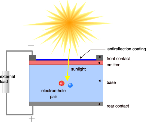
Image source: PVEducation - Solar Cell Structure
From Cell to Panel: The Architecture of a Working Solar Module
A single silicon solar cell produces only about 0.5 to 0.6 volts under open-circuit conditions—insufficient for most applications. To achieve useful voltages, cells are connected in series. A typical 60-cell panel might produce 30 to 40 volts. For higher current, cells can be connected in parallel.
The physical construction of a modern solar cell involves multiple layers engineered for both optical and electrical performance. Light enters through a transparent top layer, usually glass or transparent plastic, which protects the cell while allowing photons to pass. Beneath this lies an anti-reflective coating, typically silicon nitride, which reduces surface reflection from about 30% to less than 5%, ensuring more photons reach the active silicon.
The front surface features a grid of thin metal lines—fingers and busbars—that collect current while blocking minimal light. Modern cells use multiple thin busbars rather than fewer thick ones to reduce shading while maintaining good electrical contact. The fingers, typically 30-50 micrometers wide, collect electrons from the N-type emitter layer and deliver them to the busbars.

Image source: Wikipedia - Solar cell
The silicon wafer itself is typically 160-200 micrometers thick—about twice the width of a human hair. The N-type emitter on the front surface is only a few micrometers thick, while the P-type base constitutes most of the wafer. The back surface is covered entirely with a metal contact, usually aluminum or silver paste, which collects holes.
The Shockley-Queisser Limit: Why 33.7% Is the Ceiling
In 1961, William Shockley and Hans-Joachim Queisser published a seminal paper calculating the maximum theoretical efficiency of a single-junction solar cell under standard solar illumination. Their analysis revealed a fundamental limit of 33.7% for a material with the optimal band gap of about 1.34 eV.
This limit arises from two unavoidable loss mechanisms:
Thermalization loss: High-energy photons—those with energy significantly above the band gap—create electron-hole pairs, but any excess energy beyond the band gap is dissipated as heat. A violet photon with 3 eV of energy striking silicon produces the same electron-hole pair as a red photon with 1.1 eV. The remaining 1.9 eV becomes waste heat.
Transmission loss: Low-energy photons—those below the band gap—pass through the material without being absorbed at all. They contribute nothing to electricity generation.

Image source: Wikipedia - Shockley-Queisser limit
Silicon, with its 1.12 eV band gap, sits close enough to the optimum that single-junction cells can theoretically reach about 29.4% efficiency (lower than the 33.7% maximum because silicon’s band gap isn’t quite optimal). Real-world commercial panels achieve 22-24%, with laboratory records reaching 26.8% for single-junction silicon cells.
The remaining gap between theoretical and practical efficiency comes from additional losses: reflection from surfaces, resistive losses in the semiconductor and metal contacts, recombination of electron-hole pairs before they can be collected, and incomplete absorption of light that enters the cell.
Monocrystalline vs. Polycrystalline vs. Thin Film: The Trade-offs
Solar cell efficiency depends heavily on crystal quality. Monocrystalline silicon cells are cut from single-crystal ingots grown by the Czochralski process—a method where a seed crystal is slowly pulled from molten silicon, forming a cylindrical boule with a uniform crystal structure. Electrons can travel through this ordered lattice with minimal scattering, yielding efficiencies of 20-24% for commercial cells.
Polycrystalline cells are made from silicon that has solidified in a mold, creating multiple crystal grains with boundaries between them. These grain boundaries act as recombination centers where electrons and holes annihilate without contributing to current. Polycrystalline cells typically achieve 15-18% efficiency but cost less to manufacture.
Thin-film technologies take a different approach. Rather than cutting wafers from silicon ingots, thin-film cells deposit semiconductor materials—cadmium telluride (CdTe), copper indium gallium selenide (CIGS), or amorphous silicon—in thin layers just 1-3 micrometers thick on glass, plastic, or metal substrates. While less efficient than crystalline silicon (10-13% for commercial CdTe, up to 18% for laboratory CIGS), thin-film panels offer advantages in manufacturing cost, flexibility, and performance in low-light or high-temperature conditions.
Breaking the Limit: Tandem and Multi-Junction Cells
The Shockley-Queisser limit applies only to single-junction cells. By stacking multiple junctions with different band gaps, engineers can capture more of the solar spectrum. Each layer absorbs photons with energy matching its band gap, passing higher and lower energy photons to adjacent layers.
Silicon-perovskite tandem cells represent the most promising near-term breakthrough. Perovskite materials (named after their crystal structure, not their composition) can be engineered with band gaps of 1.6-1.8 eV—ideal for capturing visible light. Placed atop a silicon cell optimized for infrared, the combination can exceed the Shockley-Queisser limit.
In April 2025, LONGi announced a silicon-perovskite tandem cell achieving 34.85% efficiency—a record that demonstrates the viability of this approach. These tandem cells could theoretically reach 43% efficiency with further optimization.
Multi-junction cells using III-V semiconductors (gallium arsenide, indium phosphide, and related compounds) have achieved even higher efficiencies, reaching 46% under concentrated sunlight. These cells are expensive to manufacture but essential for space applications where efficiency and weight matter more than cost. The Mars rovers, for instance, use triple-junction gallium indium phosphide/gallium arsenide/germanium cells.
Temperature’s Hidden Cost
Solar panels perform best in bright light—but not in high heat. As temperature rises, the band gap of silicon decreases slightly, but more importantly, the reverse saturation current increases exponentially. The net effect reduces the open-circuit voltage by about 0.35-0.5% per degree Celsius above 25°C.
A panel rated at 400 watts under standard test conditions (25°C, 1000 W/m² irradiance) might produce only 320-340 watts on a hot summer day when the cell temperature reaches 65°C. This is why panels in cool, sunny climates like Germany often outperform panels in hot, sunny climates like Arizona on a per-watt-rated basis.
The temperature coefficient varies by cell technology. N-type silicon cells, doped with phosphorus rather than boron, show better temperature stability than traditional P-type cells. Perovskite cells have even lower temperature coefficients, making them attractive for hot climates.
The Future: Beyond Silicon
After seven decades of commercial development, silicon solar technology has matured considerably. Incremental improvements continue—better anti-reflective coatings, passivated emitter and rear cell (PERC) designs, bifacial panels that collect light from both sides—but the technology is approaching its practical limits.
Perovskite solar cells offer a potential leap forward. They can be manufactured using solution processing—essentially printing—rather than the high-temperature, energy-intensive methods required for silicon. Laboratory efficiencies have reached 27% for single-junction perovskite cells, with remarkable progress over just 15 years of development.
The challenges are durability and stability. Perovskite materials can degrade under moisture, heat, and prolonged light exposure. Commercial panels must maintain at least 80% of their initial performance for 25 years—a standard silicon panels readily meet. Solving the stability problem could unlock solar cells that are cheaper, lighter, and more efficient than anything available today.
From Becquerel’s 1839 laboratory observation to modern panels covering rooftops worldwide, the photovoltaic effect has proven to be one of humanity’s most powerful tools for harnessing energy. Each panel contains billions of P-N junctions, each one a miniature factory converting quantum interactions into usable electricity. The physics is elegant; the engineering, precise; and the impact, transformative.
References
-
Chapin, D.M., Fuller, C.S., & Pearson, G.L. (1954). “A New Silicon p-n Junction Photocell for Converting Solar Radiation into Electrical Power.” Journal of Applied Physics, 25(5), 676-677.
-
Becquerel, A.E. (1839). “Mémoire sur les effets électriques produits sous l’influence des rayons solaires.” Comptes Rendus, 9, 561-567.
-
Shockley, W., & Queisser, H.J. (1961). “Detailed Balance Limit of Efficiency of p-n Junction Solar Cells.” Journal of Applied Physics, 32(3), 510-519.
-
Wikipedia. “Solar cell.” https://en.wikipedia.org/wiki/Solar_cell
-
Wikipedia. “Theory of solar cells.” https://en.wikipedia.org/wiki/Theory_of_solar_cells
-
Wikipedia. “Shockley–Queisser limit.” https://en.wikipedia.org/wiki/Shockley%E2%80%93Queisser_limit
-
PVEducation. “Solar Cell Structure.” https://www.pveducation.org/pvcdrom/solar-cell-operation/solar-cell-structure
-
American Physical Society. “First Practical Silicon Solar Cell.” https://www.aps.org/apsnews/2009/04/bell-labs-silicon-solar-cell
-
IEEE Global History Network. “Milestones: First Practical Photovoltaic Solar Cell.” https://ethw.org/Milestones:First_Practical_Photovoltaic_Solar_Cell
-
LONGi. “34.85%! LONGi Breaks World Record for Crystalline Silicon-Perovskite Tandem Solar Cells.” https://www.longi.com/en/news/silicon-perovskite-tandem-solar-cells-new-world-efficiency/
-
National Renewable Energy Laboratory. “Best Research-Cell Efficiency Chart.” https://www.nrel.gov/pv/cell-efficiency.html
-
MIT Technology Review. “Super-efficient solar cells: 10 Breakthrough Technologies 2024.” https://www.technologyreview.com/2024/01/08/1085124/super-efficient-solar-cells-breakthrough-technologies/
-
Stanford University. “Silicon Solar Cells.” http://large.stanford.edu/courses/2015/ph240/zhao-a1/
-
Sinovoltaics. “Energy Band Gap of Solar Cells.” https://sinovoltaics.com/learning-center/solar-cells/energy-band-gap-of-solar-cells/
-
G2V Optics. “Theory of Solar Cells.” https://g2voptics.com/photovoltaics-solar-cells/photovoltaics-solar-cells/theory-of-solar-cells/
-
Energy.gov. “Solar Photovoltaic Cell Basics.” https://www.energy.gov/eere/solar/solar-photovoltaic-cell-basics
-
Fluxim. “Highest Perovskite Solar Cell Efficiencies (2026 Update).” https://www.fluxim.com/research-blogs/perovskite-silicon-tandem-pv-record-updates
-
ScienceDirect. “Overview of the Current State of Gallium Arsenide-Based Solar Cells.” https://pmc.ncbi.nlm.nih.gov/articles/PMC8200097/
-
GreenTech Renewables. “How Does Heat Affect Solar Panel Efficiencies?” https://www.greentechrenewables.com/article/how-does-heat-affect-solar-panel-efficiencies
-
Sinovoltaics. “Anti Reflective Coating for Solar Panels.” https://sinovoltaics.com/learning-center/solar-cells/anti-reflective-coating-for-solar-panels/
-
PV-Manufacturing.org. “Metallisation, More Busbars.” https://pv-manufacturing.org/teaching-resources/sunsolve-tutorials/sunsolve-5-metallisation-more-busbars/
-
Smithsonian Magazine. “A Brief History of Solar Panels.” https://www.smithsonianmag.com/sponsored/brief-history-solar-panels-180972006/